About the project
High-Density Lithium Niobate Photonic Integrated Circuits
Translating high-speed electrical signals to the optical domain, electro-optic (EO) modulators are key components of photonic systems. On a technological level, lithium niobate (LN) has become a mainstay for such devices, offering a unique combination of strong EO activity and chemical stability as well as wide-band transparency and the ability to withstand high optical power levels.
Recent advances in thin-film LN have opened an attractive path towards compact footprint, low operation voltage and large bandwidth, while maintaining the intrinsic advantages of the underlying material system. However, there is still a need to further reduce the component size and increase the component density of LN circuits to truly enable large scale photonic integration in volume over the current wafer sizes, which are still far from the 200-300 mm scale of silicon photonics. It is thus the goal of HDLN to establish an internationally unique technology base related to high-density thin-film LN technology. HDLN will demonstrate the viability of the technology platform through a series of demonstrators, geared towards highly relevant applications such as ultra-fast optical communications and ultra-wideband photonic-electronic signal processing.
HDLN brings together a careful selection of experienced partners from academia and industry, comprising a recently incorporated start-up for the manufacturing platform, an independent photonic design and test house, and an internationally leading company in the field of communications that validates the technology at the application level.
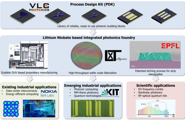
HDLN consortium aims to tackle five objectives:
Objective 1: Development of a wafer scale, ultra-low loss, DUV-based LNOI processing with the aim of commercialize the manufacturing of wafer-scale ultra-low loss PIC based on LNOI channel waveguides.
Objective 2: Development of PDK for open-access manufacturing foundry commercialization of HDLN establishing a generic fab process and its corresponding design manual and qualified component library, assembled into a process design kit (PDK) for the LNOI foundry.
Objective 3: Proving platform viability by selected application demonstrations of high impact in two highly relevant communication applications fields: Ultra-fast optical telecom/datacom transceivers and THz- and mm-wave photonics. The associated objectives are briefly described in the following.
Objective 4: Early access wafer runs (pre-PDK), market study. HDLN aims to secure early access to customers interested in engaging in NRE (non-recurrent engineering) runs with LXT based on designs acquired from academic partnerships or supplied by LXT. Objective 5: Open-access foundry level offering of LNOI integrated photonic circuits. HDLN aims to establish a commercial offering for low barrier-of-entry access to HDLN technology via a dedicated foundry service. Targeted customers range from research institutions to industrial companies and enterprises.