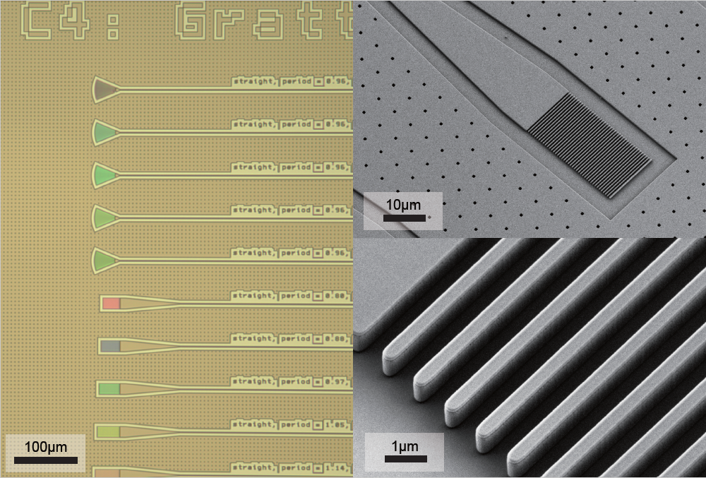
Lithium Niobate has emerged as a promising platform in the field of integrated photonics. Like other mature photonics platforms, Lithium Niobate boasts low material absorption, allowing for the development of ultra-low-loss photonics waveguides. What sets Lithium Niobate apart is its electro-optic effect, which holds immense potential to revolutionize communication, sensing, and computing technologies.
However, a major challenge for the Lithium Niobate photonics community is its chemical stability, making it difficult to etch and pattern. At EPFL, the HDLN project has addressed this challenge by developing a novel etching method using a new hard-mask material: Diamond-like Carbon. This advance has enabled us to fabricate high-quality, high-confinement Lithium Niobate waveguides with losses below 4 dB/m [publication 1].
Photonic integrated circuits are typically fragile and require protection and isolation from environmental factors. Silicon Dioxide is an ideal cladding material, but current deposition methods often suffer from hydrogen-related absorption due to the precursor used. Within HDLN, EPFL has overcome this challenge by developing a new method for silicon dioxide cladding deposition using silicon tetrachloride, a hydrogen-free precursor [publication 2]. In summary, we can now fabricate low-loss, high-confinement Lithium Niobate waveguides with high-quality silicon dioxide cladding at EPFL. This advancement enables our partners in HDLN to further explore various interesting functionalities and applications on the Lithium Niobate platform
