After the development of basic components and more advanced building blocks, the full potential of the HDLN platform was demonstrated with applications in communications and microwave photonics. We conducted data transmission experiments using intensity modulation and direct detection, as well as coherent schemes, achieving data transmission using 16-state quadrature-amplitude modulation (16QAM) at symbol rates up to 200 GBd (see Fig. 1(a)). Furthermore, we used the Mach-Zehnder modulators (MZM) developed in HDLN to convert ultra-broadband analog electrical signals with frequencies up to 325 GHz to the optical domain and perform photonic-assisted signal processing using the architecture developed in the project “TERASLICE”. Fig. 1(b) shows the spectrogram of an electrical chirp signal covering the frequency range from 220.5 GHz to 328.5 GHz, digitized with the photonic-electronic analog-to-digital converter (PE-ADC) scheme using an HDLN MZM.
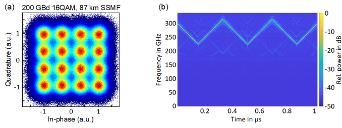
Fig. 1: Results of application demonstration using HDLN modulators. (a) Constellation diagram of the received 16-state quadrature-amplitude modulation (16QAM) at a symbol rate of 200 GBd after transmission over 87 km of standard single-mode fiber (SSMF). (b) Spectrogram of an electrical chirp signal covering the frequency range from 220.5 GHz to 328.5 GHz, digitized with the photonic-electronic analog-to-digital converter (PE-ADC) scheme.