
The HDLN PDK has been fully implemented in the GDSFactory design environment, providing a flexible, script‑based framework for photonic layout development. Through GDSFactory, users can access parameterized cells, validated component libraries, layer definitions, and automated design‑rule checks aligned with the fabrication process. This integration supports efficient circuit design, layout generation, and the reliable reuse of the validated building blocks included in the platform.
The HDLN PDK will be made available to customers upon request. Interested designers may contact LXT, which coordinates access to the PDK and provides the corresponding technical support.
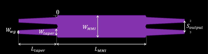
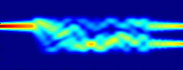
FDTD methods are used to optimize the geometry of 2×2 multimode interferometers
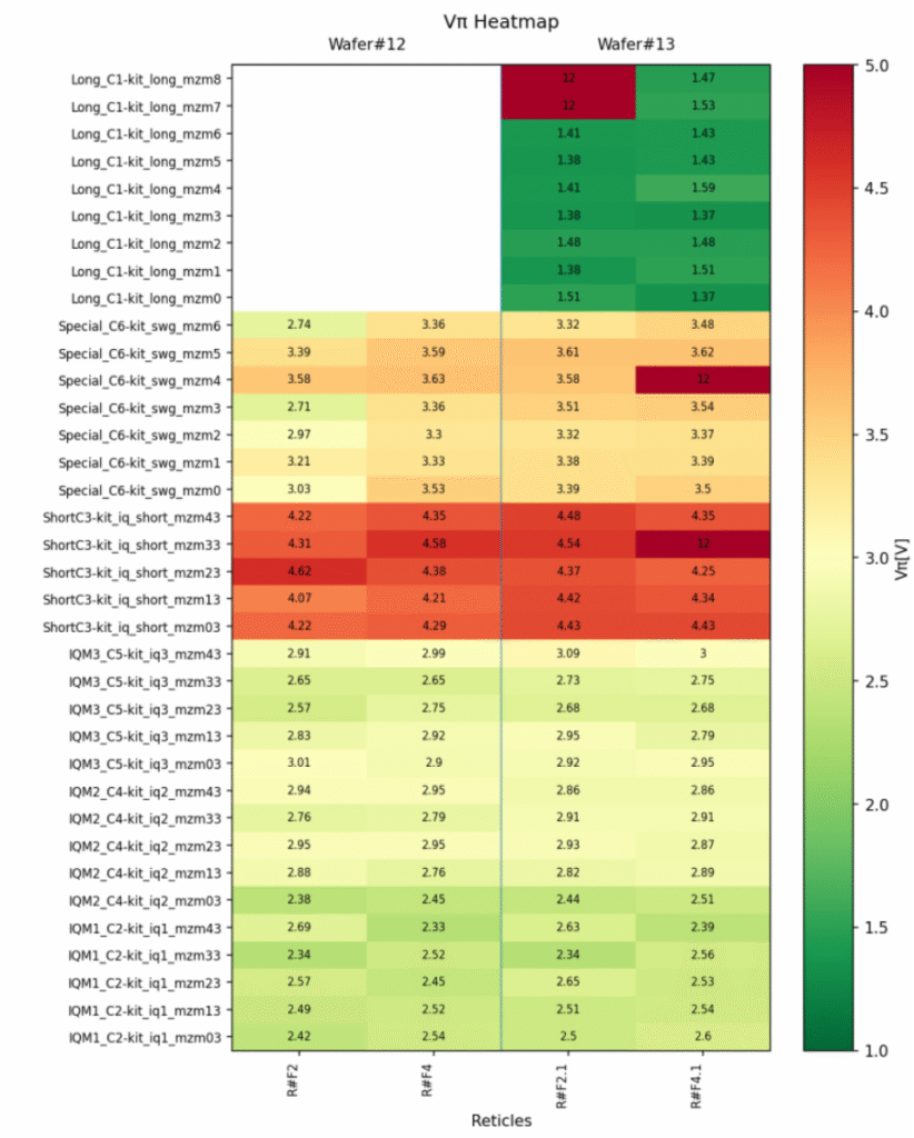
Wafer-level testing of PDK components allowed the choice of the optimal parameters for minimal insertion loss and highest modulation efficiency.
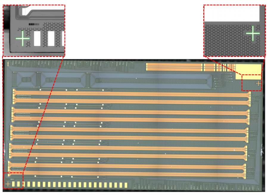
Before die-scale testing, the position and orientation of the die is adjusted with computer vision, using dedicated fiducial marks.