The deep-etched LNOI waveguides (HDLN process) developed at EPFL were successfully transferred to the spin-off company Luxtelligence for future exploitation. Luxtelligence adopted the know-how from EPFL and was responsible for the nanofabrication of the photonic devices using the HDLN process throughout the project. This resulted in the realization of verified components designed by VLC Photonics for the PDK. The verified design library was subsequently used by the consortium to design custom photonic chips, which were fabricated by Luxtelligence and characterized by both academic and industrial partners. In addition, the foundry operations were successfully established, including design compilation from multiple customers and the organization of multi-project wafer batches with yield optimization. These achievements paved the way for the future commercialization of HDLN’s unique nanofabrication technology in the targeted telecommunications and optical transceiver markets.
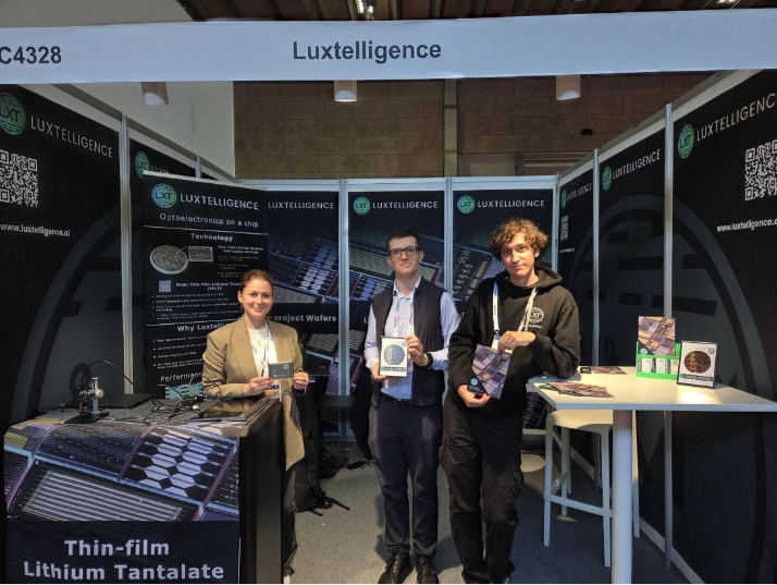
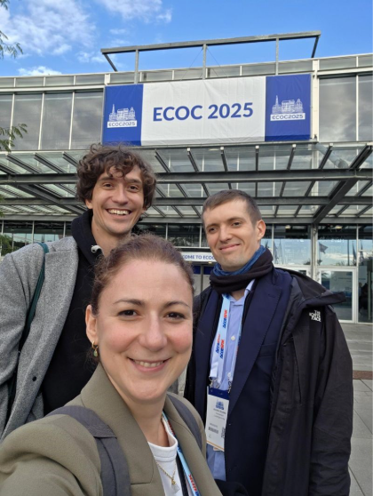
Luxtelligence actively participated in ECOC 2025, where the company showcased its TFLN and TFLT fabrication services and the HDLN technology node. The team, led by Mikhail Churaev, Alessandra Di Leo, Nick Sauerwein, and Andrei Kiselev, met with potential customers and explored opportunities to demonstrate how their technology advances the boundaries of photonic integrated circuits. The event took place from September 29 to October 1, 2025, in Copenhagen, where Luxtelligence exhibited at Stand C4328. Throughout the event, the team engaged with attendees and presented their latest innovations in photonics and optical communications.